Distinguished Professor, Department of Electrical and Computer Engineering, UCLA Mau-Chung Frank Chang
Beyond Moore’s Law
A New Semiconductor Landscape Shaped by Glass Substrates and Heterogeneous Integration
With Moore’s Law reaching its limits, heterogeneous integration has become mainstream in the semiconductor industry. By combining materials with vastly different properties into a single package, engineers are overcoming the physical limits inherent in monolithic substrates. Notably, the most significant breakthroughs are expected to come from material innovations in packaging substrates.
Currently, the mainstream CoWoS (Chip-on-Wafer-on-Substrate) packaging uses silicon wafers as interposers. However, the physical boundaries and circular geometry of a standard 12-inch wafer constrain the total number of dies and layout flexibility within a single package. In addition, silicon interposers are limited by the reticle size of photolithography tools, a constraint that prevents unlimited expansion on a single silicon substrate.
Within the next one to two years, packaging substrates are expected to shift toward glass. Drawing on display panel technology, glass substrates can scale to 65 inches, 85 inches, or even larger. This breakthrough overcomes the 12-inch wafer limitation, enabling higher-density routing and larger-scale integration. The critical challenge for glass substrates, however, lies in coefficient of thermal expansion (CTE) matching. Specialized glass must be developed with thermal expansion rates aligned to both silicon and compound semiconductors to ensure structural stability and prevent warpage.
The role of silicon is shifting in the era of heterogeneous integration. It is becoming a primary mechanical backbone rather than the sole driver of component performance. Most notably, silicon cannot emit light. By using heterogeneous integration to embed light-emitting materials such as indium phosphide (InP) or gallium nitride (GaN) directly into silicon-based circuits, chips can replace electrons with photons to enable high‑speed optical communication.
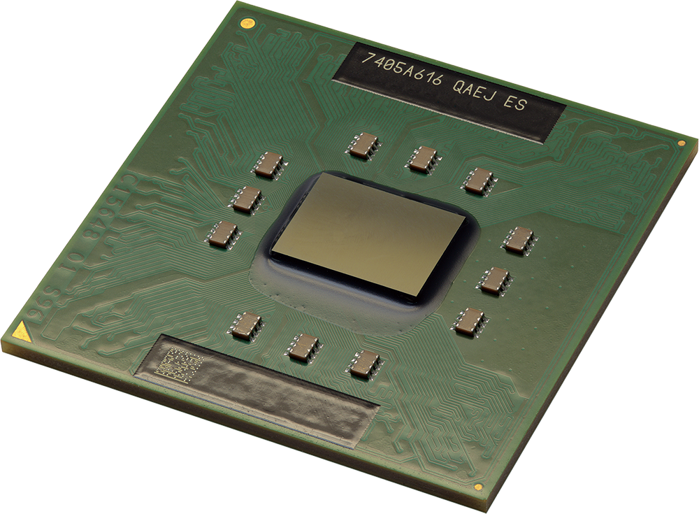
To achieve optoelectronic integration and address the efficiency and speed requirements of future AI computing, light-emitting materials such as indium phosphide (InP) or gallium nitride (GaN) will be integrated with CMOS logic circuits at the wafer level. This integration is expected to become mainstream within the next two to three years.
Currently, most packaging technologies place the laser source off-chip. However, lasers are extremely temperature-sensitive; a fluctuation of just 2℃ to 3℃ can cause severe wavelength drift and lead to communication failure. Solving this requires true on-chip optoelectronic integration, with the light source built directly into the digital circuitry. This requires embedding on-die micro‑thermometers and temperature controllers to achieve precise, localized thermal regulation, rather than relying on ambient cooling.
In the 6G and sub-terahertz era, optoelectronic integration will be pivotal. Future data transmission will move away from traditional copper interconnects, which cause severe loss and generate heat, toward lighter and more efficient media. This involves using silicon photonics for intra-chip signaling and polymer waveguides for inter-system sub-THz transmission. Although the materials used and frequencies differ, the fundamental task of data transmission remains the same. In the future, this will be achieved by replacing electrical signal transmission with optical transmission, thus harnessing the speed of light to deliver the extreme bandwidth and low latency required in the 6G era.
Traditional copper wiring is also prohibitively heavy. In robots or electric vehicles, carrying dozens of pounds of copper cabling would severely restrict mobility and efficiency. Coupled with rising copper costs driven by geopolitical pressures, replacing copper with advanced waveguides for sub-THz communication to achieve system lightweighting is the inevitable path forward.
However, silicon wafers remain highly capable of computation. Therefore, to produce the miniaturized, high-performance chips required for the 6G era, it is necessary to integrate compound semiconductors optimized for high-frequency signals with silicon logic chips that excel at logic and computation. Because 6G signals are extremely sensitive to interference and temperature variation, glass substrates provide more than just additional space. Their superior electrical insulation and precise thermal control are critical to ensuring signal stability and preventing drift.
In the semiconductor industry, failing to sustain high yields is tantamount to failing to be profitable. While technological leadership is essential, the definitive competitive edge lies in achieving commercially viable yields amid the complexity of heterogeneous integration. This helps ensure an unassailable position in the face of competition.
It is recommended that the Semiconductor Research Center adopt a best junction for the function approach. By focusing on sensors and light‑emitting components and boldly integrating compound semiconductors with optical technologies, the Center can leverage its superior system design capabilities to build a sustainable technological advantage. This approach will transform complex technical challenges into high-margin commercial opportunities, enabling it to secure an advantageous position within the global semiconductor value chain.