NYCU × Trapped-Ion Quantum Computing Laboratory Overcoming Optical Limits with Non-local Metasurfaces
Step into a traditional quantum computing laboratory, and you are immediately met with a dense jungle of steel and glass, an optical table crowded with precision lenses, mirrors, and laser arrays.
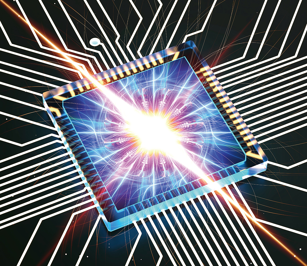
However, this familiar scene is undergoing transformation. Through the collaboration between Associate Professor You-Chia Chang’s team at the National Yang Ming Chiao Tung University (NYCU) Department of Photonics and the Trapped-Ion Quantum Computing Laboratory, massive optical systems are being miniaturized onto a silicon nitride (Si3N4) chip with a centimeter-scale footprint. This represents not merely the downsizing of optical components but also a strategic milestone in Taiwan’s transition from electronic integrated circuits (EICs) to quantum photonic integrated circuits (QPICs).
From Theoretical Exploration to Killer Applications
This cross-disciplinary collaboration stems from the precise alignment of academic foresight with industrial application needs. NYCU has long maintained a leading position in metasurfaces and nanophotonics, while the Hon Hai Research Institute focuses on building scalable ion-trap quantum computing architectures.
Ion trap quantum computers require highly collimated and precise laser beams to manipulate ion qubits, often necessitating the simultaneous control of multiple qubits. While traditional optical tables offer flexibility, they lack the spatial efficiency required for future demands involving thousands of qubits. The Laboratory provides a system-level integration perspective, enabling NYCU’s research to move from discrete components to the system level, thereby helping overcome the challenges of hardware implementation.
Technological Breakthrough: The Non-local Advantage
The centerpiece of this collaboration is the development of a non-local visible-light metasurface integrated onto a silicon nitride waveguide. Professor Chang explains that maintaining high-fidelity beam profiles at the 532 nm green light wavelength presents a formidable engineering challenge. Traditional metasurfaces rely on ultra-fine, high-aspect-ratio sub-wavelength structures to modulate optical phase; however, as wavelengths shorten, the fabrication complexity of these microstructures grows exponentially.
To overcome this challenge, Professor Chang’s team introduced a non-local design approach. Instead of confining light strictly within a single nanoscale structure, the design disperses optical fields across multiple resonators. This approach is significantly more compatible with semiconductor fabrication processes, reducing manufacturing complexity while still enabling highly precise local phase control to generate high-quality beams.
In addition, the collaboration moved away from silicon, commonly used in photonics, opting instead for silicon nitride (Si3N4). This is because silicon absorbs visible light, while silicon nitride offers excellent transparency and durability across the visible to near-infrared spectrum. Moreover, its high compatibility with existing semiconductor processes makes it the preferred material internationally for advancing ion-trap quantum computing.
Defining the Quantum Chip Ecosystem
Within this collaboration, the Hon Hai Research Institute plays an important role in defining specifications and acting as a bridge between academia and industry.
In the early stages, the teams had to mesh, having come from different fields. NYCU specialized in optical benchmarks such as waveguide loss and phase control, while the Trapped-Ion Laboratory focused on quantum metrics like qubit fidelity. By mapping these complex quantum requirements onto nanophotonic specifications, the researchers gained a clear understanding of how even minor optical deviations, such as beam misalignment or mode mismatch, directly degrade the performance of the quantum system.
The current research results, successfully demonstrated at 532 nm green light, demonstrate exceptional versatility. Because the design principles of the metasurface inherently support cross-wavelength scalability, the team plans to extend integration to red and blue light and ultimately tackle the more lossy ultraviolet regime. Their roadmap envisions consolidating multiple laser wavelengths onto a single chip platform, paving the way for comprehensive on chip spectroscopic functionality.
The collaboration sends a clear signal to the global technology sector. Leveraging its robust semiconductor supply chain, Taiwan is now equipped to enter the high-value domain of quantum photonic chips. With a fully integrated ecosystem spanning chip design, fabrication, and advanced packaging, Taiwan is positioned not only to provide foundry services but also to command the core delivery technologies of quantum systems in the coming global race.