Semiconductor Research Center Advancing Integration and Novel Materials to Reshape Next-Generation Standards
As global demand for AI computing grows exponentially and electric vehicles and renewable energy grids become ubiquitous, semiconductor innovation is no longer merely about boosting raw performance; it now requires breakthroughs in system-level integration and energy efficiency. In 2025, the Semiconductor Research Center achieved major advances across three major domains: high-speed silicon photonics, high-voltage silicon carbide (SiC), and nanophotonic integrated circuits.
Silicon Photonics: Building a Light-Speed Network in the AI Era
Today, as AI servers drive an explosive demand for bandwidth, traditional electrical signal transmission is approaching its physical limits. Once single-channel electrical transmission exceeds 100 Gbps, signal loss and interference drastically reduce communication ranges, potentially rendering data unreadable. Silicon photonics technology is the key to overcoming this barrier as it converts electrical signals into optical signals for efficient, high-performance transmission.
Developing silicon photonic chips rests on three key factors: design feasibility, scalable mass production, and rigorous testing and validation. To accelerate development, the Center has strengthened collaborations with simulation software providers and semiconductor foundries, successfully bringing its proprietary silicon photonic chip designs to fruition. In 2025, it adopted the Multi-Project Wafer (MPW) model for its initial validation phase. By allowing multiple designers to share a single wafer space area, this approach cuts development costs to just 10% of a full wafer’s price.
In addition, in 2025, the Center established an optoelectronic measurement platform supporting the 112 GBaud (224 Gb/s 4-level Pulse Amplitude Modulation, or PAM4) standard. In high-speed transmission, exceeding 200 Gbps on a single channel represents an exceptionally high threshold, which involves complex conversions from electrical to optical signals, optical transmission, and conversion back to electrical signals at the receiving end. However, this new platform can validate compliance with the PAM4 modulation standard, resolving issues of signal distortion and compensation. The establishment of this platform allows the research team to use empirical data to fine-tune chip design algorithms in real-time, effectively bridging the gap between design and manufacturing. Only after repeated iterations confirm that virtual simulations align consistently with real-world data can the entire design process be deemed accurate and reliable. The Center anticipates moving toward full-wafer tape-outs between late 2025 and 2026, offering greater latitude for design experimentation and pilot production.
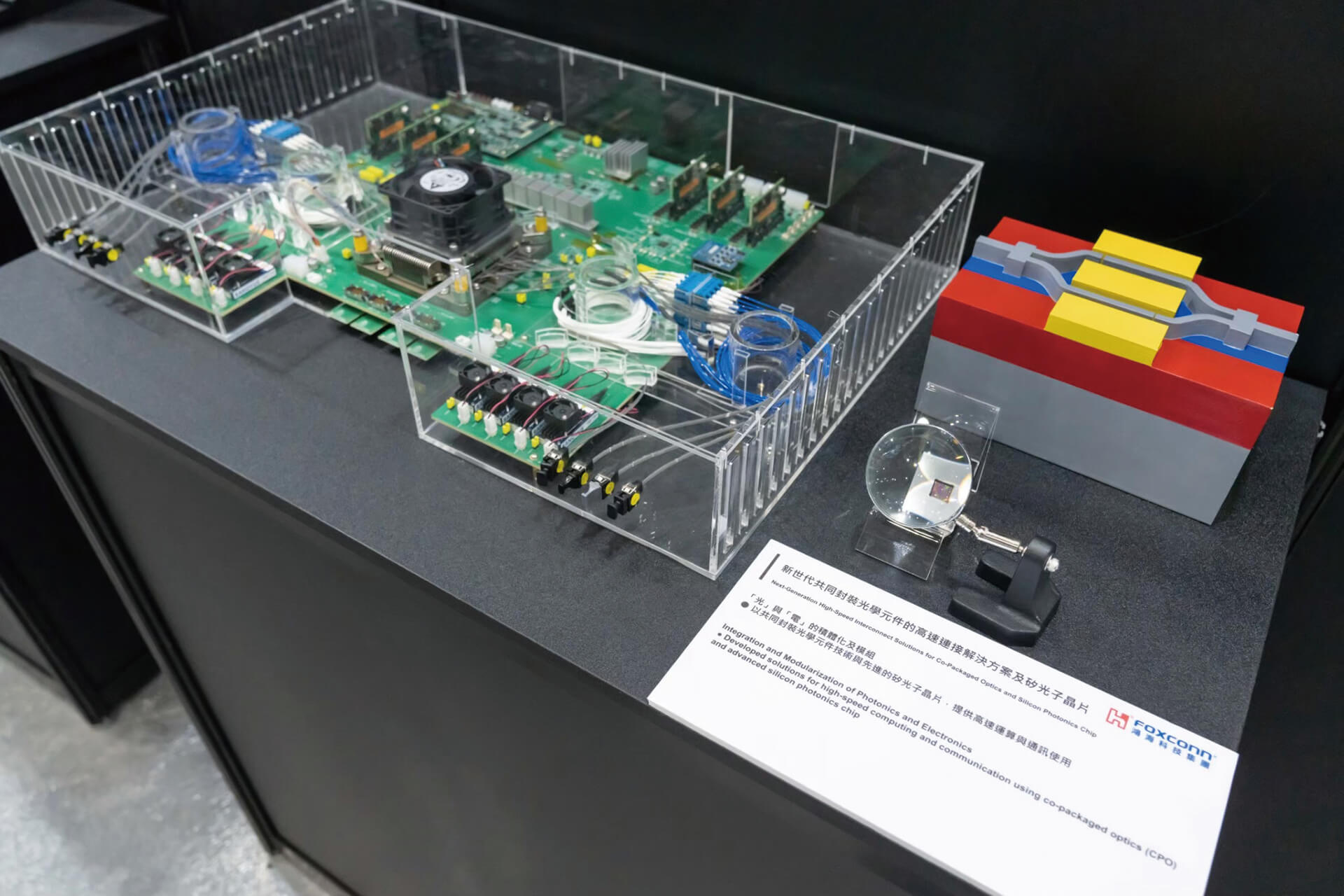
In addition to silicon-based technologies, the Center has forged a deep partnership with Delft University of Technology in the Netherlands to explore indium phosphide (InP) chips. Because silicon approaches its physical limits as single-channel speeds near 200 Gbps, achieving cleaner signals and broader bandwidths necessitates the introduction of novel physical mechanisms or materials. The jointly developed InP chips can reach a maximum single-channel transmission rate of 320 Gb/s using PAM4 modulation. Ultimately, these high-performance InP modulators and lasers will be combined with silicon photonic chips through advanced integration techniques, providing next-generation data centers with solutions that surpass the constraints of Moore’s Law.
Silicon Carbide: Driving a High-Voltage Power Revolution
If silicon photonics accelerates the communication speed of AI, silicon carbide (SiC) addresses the energy efficiency challenges of both AI and electric vehicles. As EVs migrate to 800V high-voltage platforms and the energy consumption of AI data centers soars, third-generation semiconductors, led by SiC, have become critical for energy conservation. In 2025, the Center not only achieved breakthroughs in component voltage-tolerance specifications but also took a major step forward in integration.
The 1,700V trench-type SiC devices developed by the Center are designed to meet the demanding requirements of EVs and high-power industrial applications, with primary applications in EVs, AI data centers, and high-voltage direct current (HVDC) transmission. Compared to traditional planar components, the trench design significantly reduces on-resistance. For a chip of the same area, trench devices can handle higher current densities, thereby lowering overall energy consumption.
However, the trench structure is not without its challenges. Etching a trench into the component can cause excessive electric field concentration at the bottom, which risks damaging the gate oxide layer and compromising reliability. In response, the research team developed a dual-protection approach. They created a buffer zone at the bottom using ion implantation techniques while simultaneously thickening the bottom oxide layer to withstand high voltages and keeping the current-conducting sidewalls thin. In terms of on-resistance, this achievement far exceeds the technical standards set by the National Science and Technology Council and establishes an internationally leading benchmark.
As for ultra-high-voltage scenarios, the Center has successfully developed 6,500V planar SiC devices. This technology is primarily targeted at national-level power grids and large-scale AI energy systems. In the future, hyperscale AI data centers may require dedicated substations to convert ultra-high-voltage power into medium or low voltage. During this process, the 6,500V SiC planar devices are exceptionally well-equipped to perform high-efficiency conversion and switching functions, thereby minimizing transmission losses.
In addition, traditional silicon chips fail at 150°C due to current leakage, necessitating complex heat dissipation and protection circuits. The SiC monolithic integrated circuit, developed in collaboration with National Yang Ming Chiao Tung University, overcomes this limitation to achieve stable operation in environments up to 300°C.
The core advantage of this technology lies in simplifying complexity. By directly integrating the driver circuit and power components onto the same SiC chip, it eliminates the impedance and inductance associated with traditional wire-bonding packaging. This results in faster system response times and a smaller overall footprint.
These SiC chips do not require complex cooling mechanisms and can maintain an operating frequency of 200 kHz even at high temperatures. This not only reduces the chip area by 20% to 30% but also opens entirely new frontiers for aerospace applications, deep-well drilling, and next-generation industrial control. This achievement has already been presented at the International Symposium on Power Semiconductor Devices and ICs (ISPSD), a premier academic conference in the field of power electronics.
Nanophotonics: Reshaping 3D Sensing Technology
Having mastered speed and power, the Center turned its focus toward perception. In the field of smart devices and robotics, 3D sensing technology is central to a machine’s spatial understanding. However, existing systems are bulky and power-hungry, making further miniaturization exceedingly difficult. Defying these constraints, the Center achieved a world first in 2025 with the monolithic integration of a metasurface and a Photonic Crystal Surface-Emitting Laser (PCSEL).
The current mainstream sensing light source in the market is the Vertical-Cavity Surface-Emitting Laser (VCSEL), but it suffers from inherent bottlenecks such as a large divergence angle and difficulties in developing longer wavelengths. Consequently, the Center opted for the more technically demanding PCSEL. By utilizing the nano-hole structure of photonic crystals to generate resonance, the PCSEL produces a small divergence angle to yield almost perfectly collimated light. Its spectrum is also exceptionally narrow, which eliminates the need for an additional collimating lens and thereby addresses the volume issue at its source.
Quick Glossary
Monocular Stereo Vision
A computer vision technology that uses a single camera image and AI algorithms to estimate object distances and spatial structures, thereby reconstructing a 3D scene.
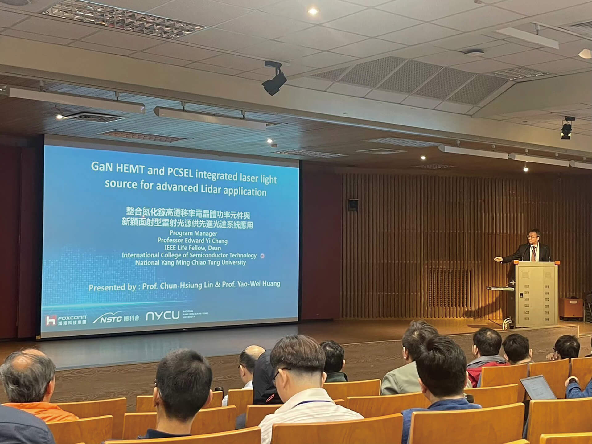
Traditional optical systems require collaboration among laser manufacturers, lens makers, and coating factories in order to stack multiple layers of optical components to generate a specific beam (such as the structured light dot projector used in Face ID). Through the Center’s research, all these functions have been integrated into a single chip. This reduces the overall module volume by a factor of 2,480 and cuts energy consumption to just 70% of conventional solutions. In addition, the entire process is completed within a semiconductor fabrication plant, eliminating lens procurement and the complexities of optical alignment and packaging.
This technology provides robust momentum for monocular stereo vision. Currently, smartphone sensors, such as the front camera notch, remain on the millimeter scale. However, the integrated single-chip component measures only about 300 micrometers, roughly the width of three human hairs. If adopted in the future, the sensor could be completely hidden within the screen bezel. This breakthrough was featured in leading international journals, including ACS Photonics and Nano Letters, and it received the Gold Award in the I-Zone Innovation Display Zone at Touch Taiwan, one of the world’s most influential display industry exhibitions. Looking ahead to future wavelength selections, the Center has also developed 1,350-nm and 1,550-nm long-wavelength components that are eye-safe. Long-wavelength lasers are easily absorbed by water and will not penetrate the eye to damage the retina, safely allowing for longer sensing distances and higher power outputs.
Looking back at the Center’s R&D advancements in 2025, despite spanning different domains, their core logic remains highly consistent. Through advanced integration and material innovation, they addressed the fundamental limitations of traditional systems: large size, high energy consumption, and slow transmission. Moving forward, the silicon photonics platform will enter the full-wafer tape-out phase, and SiC chips and PCSEL technology will undergo further optimization. The Center will continue to serve as a pivotal force, driving holistic progress in the era of AI and electric vehicles.